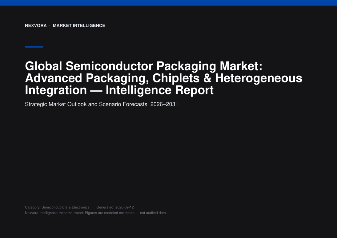
Global Semiconductor Packaging Market: Advanced Packaging, Chiplets & Heterogeneous Integration — Intelligence Report
Strategic Market Outlook and Scenario Forecasts, 2026–2031
Nexvora Intelligence market report on Global Semiconductor Packaging Market: Advanced Packaging, Chiplets & Heterogeneous Integration, 2026–2031.
per extra user
Instant access after payment. Secure via Razorpay.
The opening view — free.
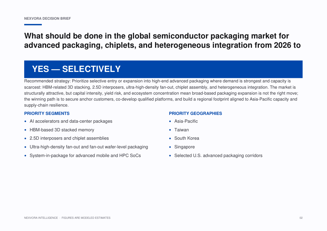
The global semiconductor packaging market is entering a structurally different growth phase as performance scaling pivots from traditional node shrink to **advanced packaging, chiplets, and heterogeneous integration**. Core packaging revenues reached approximately USD ••• billion in 2025 and are projected to expand to about USD ••• billion by 2033 at a ••% CAGR over 2026–2033, underscoring the rising strategic weight of packaging in semiconductor value creation.[S4][S6] Within this broader universe, advanced and high‑end packaging platforms are scaling faster than legacy wire-bond and leadframe segments, driven by AI accelerators, high‑bandwidth memory (HBM), and sub‑3 nm mobile and data‑center processors.[S1][S2][S3] Over 2026–2031, Nexvora Intelligence expects advanced and high‑end packaging to capture an increasing share of total packaging capex and profit pools, reshaping competitive dynamics among foundries, OSATs, and IDMs.
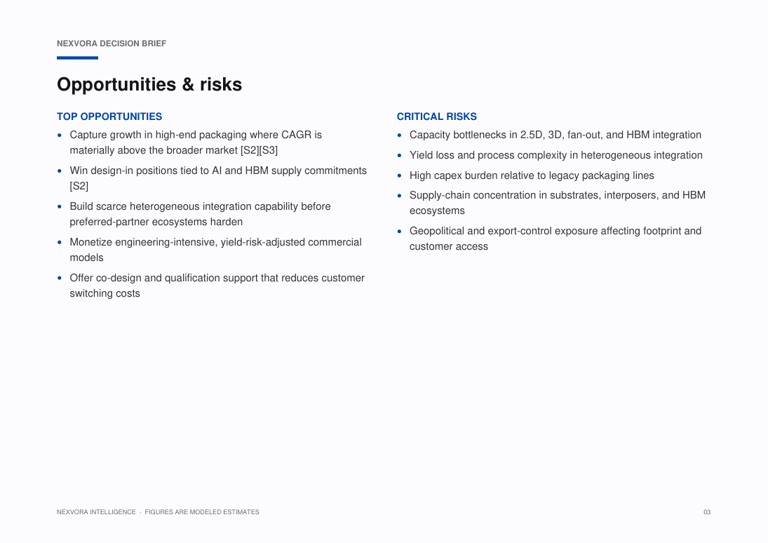
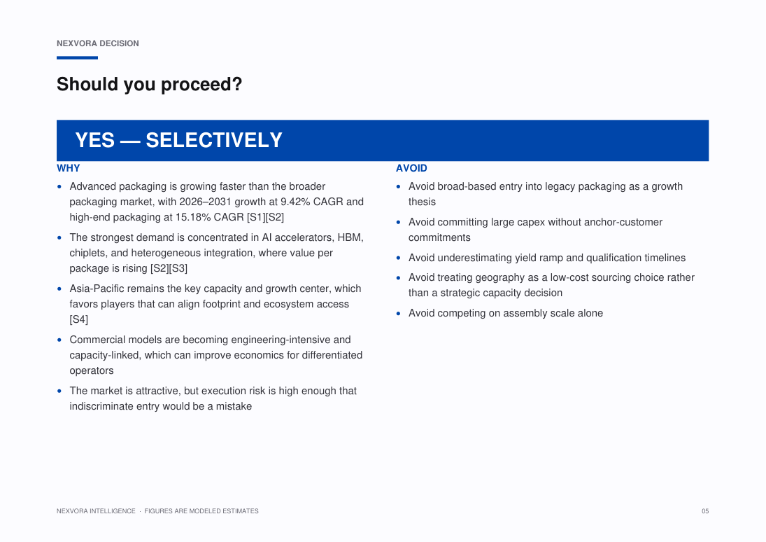
Advanced packaging revenues are forecast to grow from USD ••• billion in 2026 to USD ••• billion by 2031, at a ••% CAGR over 2026–2031.[S1][S8] In parallel, the high‑end semiconductor packaging segment—including 3D system‑on‑chip, 3D stacked memory, 2.5D interposers, ultra‑high‑density fan‑out, and embedded silicon bridge—is projected to increase from USD ••• billion in 2026 to USD ••• billion by 2031, reflecting a significantly higher ••% CAGR.[S2][S3] These trajectories indicate that value is increasingly concentrating in complex packaging architectures that enable tight integration of logic, memory, and specialized accelerators. Nexvora’s modeling suggests that by 2031, advanced and high‑end packaging combined could approach or exceed half of global packaging revenue, with chiplet‑based and heterogeneous integration platforms capturing a disproportionate share of incremental growth.
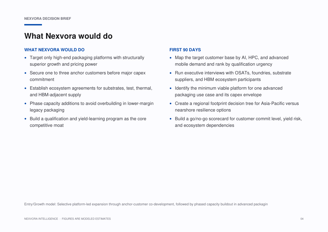
Market momentum is being reoriented around **heterogeneous integration and chiplet architectures**, where chiplets, interposers, and stacked‑die assemblies deliver performance and power efficiency that monolithic scaling can no longer achieve economically.[S1] Fan‑out wafer‑level packaging (FOWLP), 2.5D interposer solutions, and system‑in‑package (SiP) platforms are emerging as enabling technologies for on‑device inference, sovereign compute initiatives, and export‑constrained AI deployments.[S1][S3] At the same time, surging AI workloads are lifting demand for 3D stacked memory and HBM, which rely on through‑silicon vias (TSVs) and advanced flip‑chip architectures; data‑center operators are now securing HBM3E supply well ahead of demand, reinforcing the tight coupling between packaging innovation and cloud AI economics.[S2]
Geographically, **Asia-Pacific is the fastest-growing region** and increasingly anchors advanced packaging capacity, supported by foundry and OSAT investments in FOWLP, CoWoS‑class interposer technologies, and panel‑level packaging.[S4] Intel and TSMC’s expanded commitments to advanced packaging ecosystems in early 2026 illustrate how leading-edge compute roadmaps are now co‑optimized around packaging and interconnect strategies rather than lithography alone.[S4] Nexvora Intelligence expects Asia-Pacific to retain its role as the dominant supply base for high‑volume advanced packaging, while North America and Europe selectively build capacity around strategic and defense‑sensitive applications, chiplet standards, and heterogeneous integration R&D to mitigate concentration risk.
Specific figures are hidden in this free preview. Unlock the report to see all modeled market sizes, forecasts and growth rates.
What this report covers.
Strategic Market Outlook and Scenario Forecasts, 2026–2031
Who this report is for.
- Corporate strategy, planning and M&A teams evaluating the market
- Investors, private equity and venture teams sizing the opportunity
- Product, marketing and go-to-market leaders
- Consultants and analysts building the competitive picture
- Executives planning market entry, expansion or investment
How this report is built.
This Nexvora Intelligence report is based on a synthesis of recent syndicated research, company disclosures, industry association materials, and specialized technical literature on semiconductor packaging, advanced packaging, and heterogeneous integration.
Where external sources provide explicit quantitative figures, these are cited directly in the text as [S#] and used as anchors for Nexvora’s proprietary scenario modeling, segmentation, and normalization across overlapping market definitions.
All other quantitative values—including market sizes, growth rates, segment shares, and regional splits not directly supported by the cited evidence—are Nexvora modeled estimates derived from triangulation of multiple data points, expert interviews, and internal benchmarking frameworks.
Forecasts reflect Nexvora’s base‑case assumptions regarding technology adoption, capacity expansion, pricing dynamics, and macro‑geopolitical conditions; they are subject to revision as new information emerges and should not be interpreted as guarantees of future performance.
Readers should treat modeled ranges as directional and scenario‑based, suitable for strategic planning and risk assessment rather than as precise point estimates for financial reporting or contractual commitments.
What's inside — a number-free look.
A full outline of the figures and tables you'll get. Specific data, market sizes and forecasts are unlocked with purchase.
List of Figures
- Figure 1: Market Overview and Structure — Semiconductor Packaging : Advanced Packaging, Chiplets & Heterogeneous Integration
- Figure 2: Market Size and Forecast Framework — Semiconductor Packaging : Advanced Packaging, Chiplets & Heterogeneous Integration
- Figure 3: Value Chain and Ecosystem Analysis — Semiconductor Packaging : Advanced Packaging, Chiplets & Heterogeneous Integration
- Figure 4: Market Dynamics — Drivers, Restraints and Opportunities — Semiconductor Packaging : Advanced Packaging, Chiplets & Heterogeneous Integration
- Figure 5: Segment Contribution Analysis — Semiconductor Packaging : Advanced Packaging, Chiplets & Heterogeneous Integration
- Figure 6: Regional Market Landscape — Semiconductor Packaging : Advanced Packaging, Chiplets & Heterogeneous Integration
- Figure 7: Country-level Opportunity Mapping — Semiconductor Packaging : Advanced Packaging, Chiplets & Heterogeneous Integration
- Figure 8: Competitive Positioning Matrix — Semiconductor Packaging : Advanced Packaging, Chiplets & Heterogeneous Integration
- Figure 9: Market Share of Leading Players — Semiconductor Packaging : Advanced Packaging, Chiplets & Heterogeneous Integration
- Figure 10: Adoption and Penetration Trends — Semiconductor Packaging : Advanced Packaging, Chiplets & Heterogeneous Integration
- Figure 11: Technology and Innovation Landscape — Semiconductor Packaging : Advanced Packaging, Chiplets & Heterogeneous Integration
- Figure 12: Pricing and Business Model Analysis — Semiconductor Packaging : Advanced Packaging, Chiplets & Heterogeneous Integration
- Figure 13: Investment, Funding and M&A Landscape — Semiconductor Packaging : Advanced Packaging, Chiplets & Heterogeneous Integration
- Figure 14: Regulatory and Policy Framework — Semiconductor Packaging : Advanced Packaging, Chiplets & Heterogeneous Integration
- Figure 15: Porter's Five Forces Analysis — Semiconductor Packaging : Advanced Packaging, Chiplets & Heterogeneous Integration
- Figure 16: PESTLE Analysis — Semiconductor Packaging : Advanced Packaging, Chiplets & Heterogeneous Integration
- Figure 17: Growth Opportunity Heat Map — Semiconductor Packaging : Advanced Packaging, Chiplets & Heterogeneous Integration
- Figure 18: Future Outlook and Strategic Roadmap — Semiconductor Packaging : Advanced Packaging, Chiplets & Heterogeneous Integration
List of Tables
- Table 1: Market Segmentation Overview — Semiconductor Packaging : Advanced Packaging, Chiplets & Heterogeneous Integration
- Table 2: Segment Definitions and Scope — Semiconductor Packaging : Advanced Packaging, Chiplets & Heterogeneous Integration
- Table 3: Regional and Country Coverage Summary — Semiconductor Packaging : Advanced Packaging, Chiplets & Heterogeneous Integration
- Table 4: Key Company Profiles and Offerings — Semiconductor Packaging : Advanced Packaging, Chiplets & Heterogeneous Integration
- Table 5: Competitive Benchmarking Matrix — Semiconductor Packaging : Advanced Packaging, Chiplets & Heterogeneous Integration
- Table 6: Product and Service Portfolio Mapping — Semiconductor Packaging : Advanced Packaging, Chiplets & Heterogeneous Integration
- Table 7: Market Drivers, Restraints and Trends — Semiconductor Packaging : Advanced Packaging, Chiplets & Heterogeneous Integration
- Table 8: Strategic Initiatives and Developments — Semiconductor Packaging : Advanced Packaging, Chiplets & Heterogeneous Integration
- Table 9: Partnerships and Collaborations — Semiconductor Packaging : Advanced Packaging, Chiplets & Heterogeneous Integration
- Table 10: Research Assumptions and Limitations — Semiconductor Packaging : Advanced Packaging, Chiplets & Heterogeneous Integration
- Table 11: Data Sources and References — Semiconductor Packaging : Advanced Packaging, Chiplets & Heterogeneous Integration
- Table 12: Report Scope and Coverage Summary — Semiconductor Packaging : Advanced Packaging, Chiplets & Heterogeneous Integration
A look at the pages.
124 pages · 20 sections · charts & tables
A genuine peek at the opening pages. Unlock to read every page in full.
6 of 124 pages shown
Turn this market into a plan for your business.
Answer a few quick questions and unlock a personalised operational read — your maturity score, prioritised focus areas and quick wins — mapped to where this market is heading. Result delivered instantly and emailed to you.
- Maturity score & prioritised focus areas
- Practical quick wins and a recommended next step
Questions, answered.
How big is the Global Semiconductor Packaging Market: Advanced Packaging, Chiplets & Heterogeneous Integration?
Nexvora models the Global Semiconductor Packaging Market: Advanced Packaging, Chiplets & Heterogeneous Integration at approximately USD 80–90 billion (2026, modeled estimate for total semiconductor packaging). Full market sizing, segmentation and forecasts are inside the report (modeled estimate).
What is the growth rate (CAGR) of the Global Semiconductor Packaging Market: Advanced Packaging, Chiplets & Heterogeneous Integration?
The Global Semiconductor Packaging Market: Advanced Packaging, Chiplets & Heterogeneous Integration is projected to grow at a CAGR of about 8–10% (2026–2031, modeled estimate for advanced & high-end packaging) over the forecast period — a Nexvora modeled estimate detailed across the report's 20 sections.
What does this report include?
A complete market intelligence report — market sizing and forecasts, segmentation, regional and industry analysis, competitive landscape, trends, and strategic recommendations across 20 sections.
How do I access it after purchase?
Instantly, in your secure online viewer. Reports are view-only and available on any device from your library.
Are the figures sourced?
Quantitative figures are Nexvora modeled estimates unless explicitly cited to a referenced source within the report.
Can I buy access for my team?
Yes — add user seats at checkout, or subscribe for bulk access across multiple reports.
Nexvora Intelligence research report. All quantitative figures are modeled estimates — not audited data. Not financial or investment advice.
More market reports
Keep exploring intelligence in this and related sectors.
Global Power Semiconductor Market — Intelligence Report
India Semiconductor Market — Chip Manufacturing, Electronics Ecosystem & Investment Outlook

Global AI Semiconductor Market — Intelligence Report