
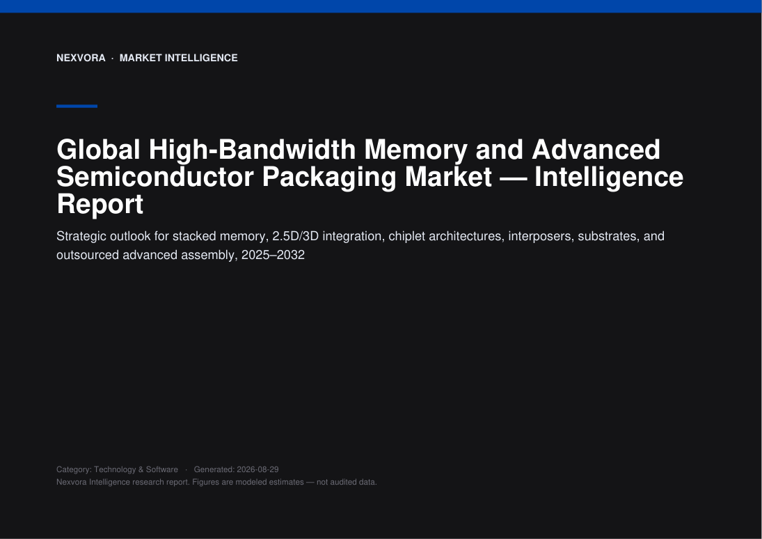
Global High-Bandwidth Memory and Advanced Semiconductor Packaging Market — Intelligence Report
Strategic outlook for stacked memory, 2.5D/3D integration, chiplet architectures, interposers, substrates, and outsourced advanced assembly, 2025–2032
Nexvora Intelligence market report on Global High-Bandwidth Memory and Advanced Semiconductor Packaging Market.
per extra user
Instant access after payment. Secure via Razorpay.
The opening view — free.
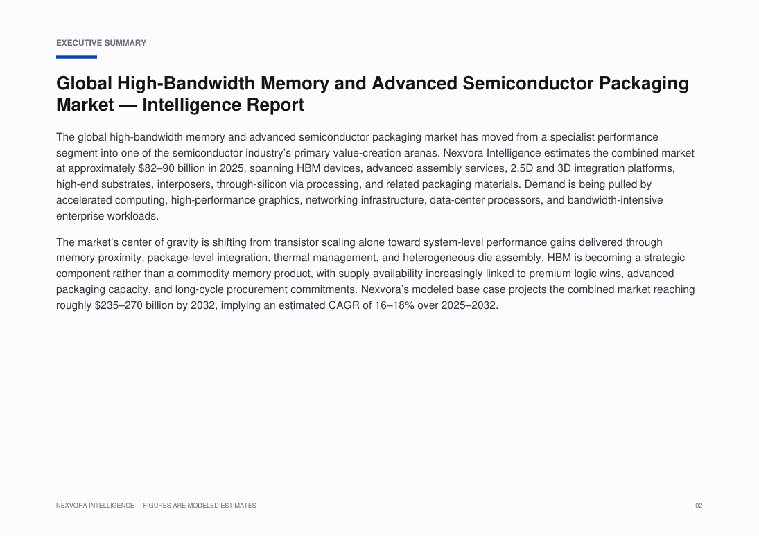
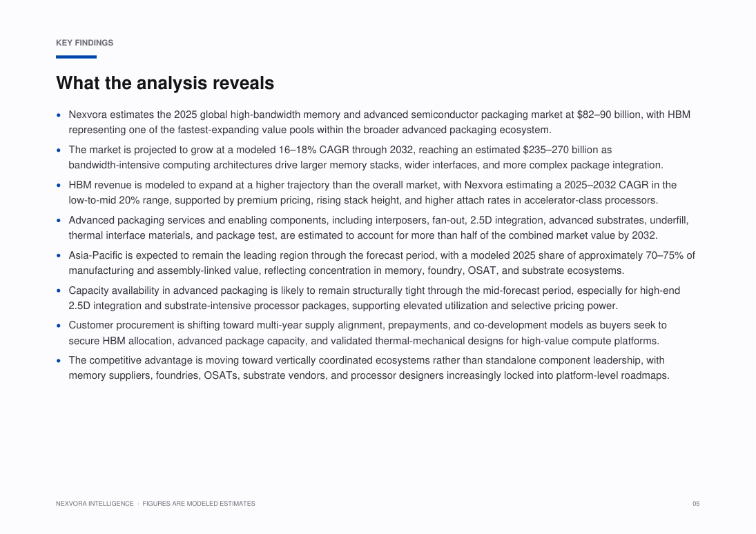
The global high-bandwidth memory and advanced semiconductor packaging market has moved from a specialist performance segment into one of the semiconductor industry’s primary value-creation arenas. Nexvora Intelligence estimates the combined market at approximately $•••–••• billion in 2025, spanning HBM devices, advanced assembly services, 2.5D and 3D integration platforms, high-end substrates, interposers, through-silicon via processing, and related packaging materials. Demand is being pulled by accelerated computing, high-performance graphics, networking infrastructure, data-center processors, and bandwidth-intensive enterprise workloads.
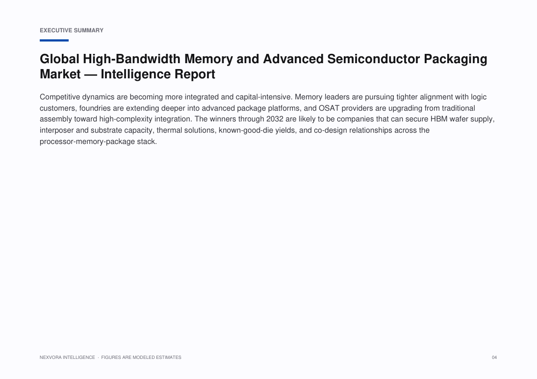
The market’s center of gravity is shifting from transistor scaling alone toward system-level performance gains delivered through memory proximity, package-level integration, thermal management, and heterogeneous die assembly. HBM is becoming a strategic component rather than a commodity memory product, with supply availability increasingly linked to premium logic wins, advanced packaging capacity, and long-cycle procurement commitments. Nexvora’s modeled base case projects the combined market reaching roughly $•••–••• billion by 2032, implying an estimated CAGR of 16–••% over 2025–2032.
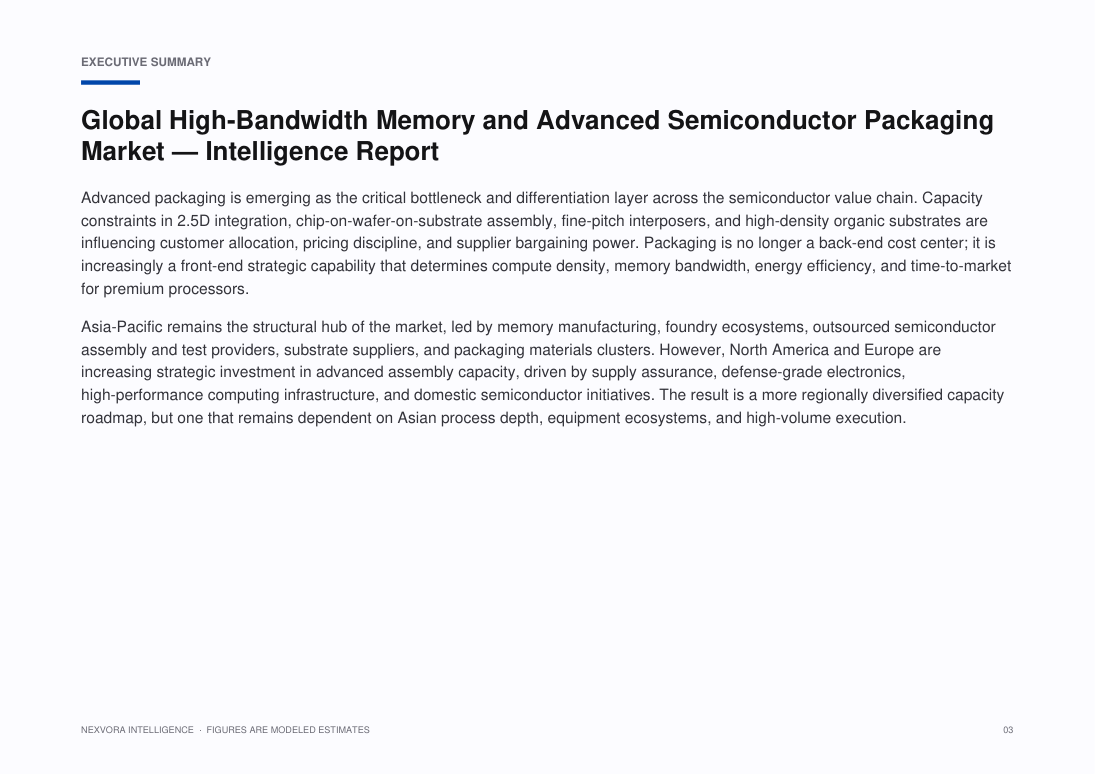
Advanced packaging is emerging as the critical bottleneck and differentiation layer across the semiconductor value chain. Capacity constraints in 2.5D integration, chip-on-wafer-on-substrate assembly, fine-pitch interposers, and high-density organic substrates are influencing customer allocation, pricing discipline, and supplier bargaining power. Packaging is no longer a back-end cost center; it is increasingly a front-end strategic capability that determines compute density, memory bandwidth, energy efficiency, and time-to-market for premium processors.
Asia-Pacific remains the structural hub of the market, led by memory manufacturing, foundry ecosystems, outsourced semiconductor assembly and test providers, substrate suppliers, and packaging materials clusters. However, North America and Europe are increasing strategic investment in advanced assembly capacity, driven by supply assurance, defense-grade electronics, high-performance computing infrastructure, and domestic semiconductor initiatives. The result is a more regionally diversified capacity roadmap, but one that remains dependent on Asian process depth, equipment ecosystems, and high-volume execution.
Specific figures are hidden in this free preview. Unlock the report to see all modeled market sizes, forecasts and growth rates.
What this report covers.
Strategic outlook for stacked memory, 2.5D/3D integration, chiplet architectures, interposers, substrates, and outsourced advanced assembly, 2025–2032
Who this report is for.
- Corporate strategy, planning and M&A teams evaluating the market
- Investors, private equity and venture teams sizing the opportunity
- Product, marketing and go-to-market leaders
- Consultants and analysts building the competitive picture
- Executives planning market entry, expansion or investment
How this report is built.
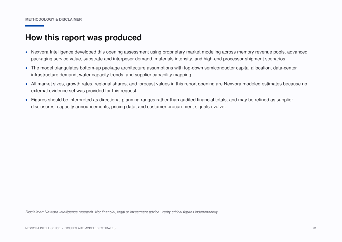
Nexvora Intelligence developed this opening assessment using proprietary market modeling across memory revenue pools, advanced packaging service value, substrate and interposer demand, materials intensity, and high-end processor shipment scenarios.
The model triangulates bottom-up package architecture assumptions with top-down semiconductor capital allocation, data-center infrastructure demand, wafer capacity trends, and supplier capability mapping.
All market sizes, growth rates, regional shares, and forecast values in this report opening are Nexvora modeled estimates because no external evidence set was provided for this request.
Figures should be interpreted as directional planning ranges rather than audited financial totals, and may be refined as supplier disclosures, capacity announcements, pricing data, and customer procurement signals evolve.
What's inside — a number-free look.
A full outline of the figures and tables you'll get. Specific data, market sizes and forecasts are unlocked with purchase.
List of Figures
- Figure 1: Market Overview and Structure — High-Bandwidth Memory and Advanced Semiconductor Packaging
- Figure 2: Market Size and Forecast Framework — High-Bandwidth Memory and Advanced Semiconductor Packaging
- Figure 3: Value Chain and Ecosystem Analysis — High-Bandwidth Memory and Advanced Semiconductor Packaging
- Figure 4: Market Dynamics — Drivers, Restraints and Opportunities — High-Bandwidth Memory and Advanced Semiconductor Packaging
- Figure 5: Segment Contribution Analysis — High-Bandwidth Memory and Advanced Semiconductor Packaging
- Figure 6: Regional Market Landscape — High-Bandwidth Memory and Advanced Semiconductor Packaging
- Figure 7: Country-level Opportunity Mapping — High-Bandwidth Memory and Advanced Semiconductor Packaging
- Figure 8: Competitive Positioning Matrix — High-Bandwidth Memory and Advanced Semiconductor Packaging
- Figure 9: Market Share of Leading Players — High-Bandwidth Memory and Advanced Semiconductor Packaging
- Figure 10: Adoption and Penetration Trends — High-Bandwidth Memory and Advanced Semiconductor Packaging
- Figure 11: Technology and Innovation Landscape — High-Bandwidth Memory and Advanced Semiconductor Packaging
- Figure 12: Pricing and Business Model Analysis — High-Bandwidth Memory and Advanced Semiconductor Packaging
- Figure 13: Investment, Funding and M&A Landscape — High-Bandwidth Memory and Advanced Semiconductor Packaging
- Figure 14: Regulatory and Policy Framework — High-Bandwidth Memory and Advanced Semiconductor Packaging
- Figure 15: Porter's Five Forces Analysis — High-Bandwidth Memory and Advanced Semiconductor Packaging
- Figure 16: PESTLE Analysis — High-Bandwidth Memory and Advanced Semiconductor Packaging
- Figure 17: Growth Opportunity Heat Map — High-Bandwidth Memory and Advanced Semiconductor Packaging
- Figure 18: Future Outlook and Strategic Roadmap — High-Bandwidth Memory and Advanced Semiconductor Packaging
List of Tables
- Table 1: Market Segmentation Overview — High-Bandwidth Memory and Advanced Semiconductor Packaging
- Table 2: Segment Definitions and Scope — High-Bandwidth Memory and Advanced Semiconductor Packaging
- Table 3: Regional and Country Coverage Summary — High-Bandwidth Memory and Advanced Semiconductor Packaging
- Table 4: Key Company Profiles and Offerings — High-Bandwidth Memory and Advanced Semiconductor Packaging
- Table 5: Competitive Benchmarking Matrix — High-Bandwidth Memory and Advanced Semiconductor Packaging
- Table 6: Product and Service Portfolio Mapping — High-Bandwidth Memory and Advanced Semiconductor Packaging
- Table 7: Market Drivers, Restraints and Trends — High-Bandwidth Memory and Advanced Semiconductor Packaging
- Table 8: Strategic Initiatives and Developments — High-Bandwidth Memory and Advanced Semiconductor Packaging
- Table 9: Partnerships and Collaborations — High-Bandwidth Memory and Advanced Semiconductor Packaging
- Table 10: Research Assumptions and Limitations — High-Bandwidth Memory and Advanced Semiconductor Packaging
- Table 11: Data Sources and References — High-Bandwidth Memory and Advanced Semiconductor Packaging
- Table 12: Report Scope and Coverage Summary — High-Bandwidth Memory and Advanced Semiconductor Packaging
A look at the pages.
88 pages · 20 sections · charts & tables
A genuine peek at the opening pages. Unlock to read every page in full.
6 of 88 pages shown
Turn this market into a plan for your business.
Answer a few quick questions and unlock a personalised operational read — your maturity score, prioritised focus areas and quick wins — mapped to where this market is heading. Result delivered instantly and emailed to you.
- Maturity score & prioritised focus areas
- Practical quick wins and a recommended next step
Questions, answered.
How big is the Global High-Bandwidth Memory and Advanced Semiconductor Packaging Market?
Nexvora models the Global High-Bandwidth Memory and Advanced Semiconductor Packaging Market at approximately $82–90 billion, 2025E. Full market sizing, segmentation and forecasts are inside the report (modeled estimate).
What is the growth rate (CAGR) of the Global High-Bandwidth Memory and Advanced Semiconductor Packaging Market?
The Global High-Bandwidth Memory and Advanced Semiconductor Packaging Market is projected to grow at a CAGR of about 16–18%, 2025–2032E over the forecast period — a Nexvora modeled estimate detailed across the report's 20 sections.
What does this report include?
A complete market intelligence report — market sizing and forecasts, segmentation, regional and industry analysis, competitive landscape, trends, and strategic recommendations across 20 sections.
How do I access it after purchase?
Instantly, in your secure online viewer. Reports are view-only and available on any device from your library.
Are the figures sourced?
Quantitative figures are Nexvora modeled estimates unless explicitly cited to a referenced source within the report.
Can I buy access for my team?
Yes — add user seats at checkout, or subscribe for bulk access across multiple reports.
Nexvora Intelligence research report. All quantitative figures are modeled estimates — not audited data. Not financial or investment advice.
Digital Twin Software vs Gallium Nitride Power Devices
Choose Digital Twin Software if you need industrial digital twin or virtual twin software tied to Dassault Systèmes’ 3DEXPERIENCE platform and applications such as CATIA, SIMULIA, DELMIA, and ENOVIA. Choose Gallium Nitride Power Devices if you need gallium nitride-based power devices in the semiconductors and electronics category. The right choice depends entirely on whether the buyer is looking for industrial software capabilities or semiconductor power devices.
Grounded in published specifications — guidance, not an endorsement.
More market reports
Keep exploring intelligence in this and related sectors.

Global Post-Quantum Cryptography Migration Services Market — Intelligence Report
Global Accelerator Memory Chips & High-Bandwidth Memory Supply Chain Market — Intelligence Report

Global Agentic Enterprise Workflow Automation Platforms Market — Intelligence Report

Global Inference ASICs & Edge Accelerator Chips Market — Intelligence Report
AI Analyst
Insights and answers generated live from Global High-Bandwidth Memory and Advanced Semiconductor Packaging Market — Intelligence Report's verified data. Modeled estimates — not investment advice.
- The report covers the Global High-Bandwidth Memory and Advanced Semiconductor Packaging Market within the Technology & Software sector.
- The strategic outlook spans 2025–2032 for stacked memory, 2.5D/3D integration, chiplet architectures, interposers, substrates, and outsourced advanced assembly.
- The market scope combines high-bandwidth memory with advanced semiconductor packaging technologies and services.
- Notable: The report emphasizes packaging-led semiconductor innovation, including chiplets and 2.5D/3D integration, alongside memory stacking.