
Global Advanced Semiconductor Packaging, Chiplet Integration and 2.5D/3D Interconnect Market — Intelligence Report
Strategic market outlook for high-density packaging architectures, heterogeneous integration and next-generation interconnect platforms, 2025–2032
Nexvora Intelligence market report on Global Advanced Semiconductor Packaging, Chiplet Integration and 2.5D/3D Interconnect Market.
per extra user
Instant access after payment. Secure via Razorpay.
The opening view — free.
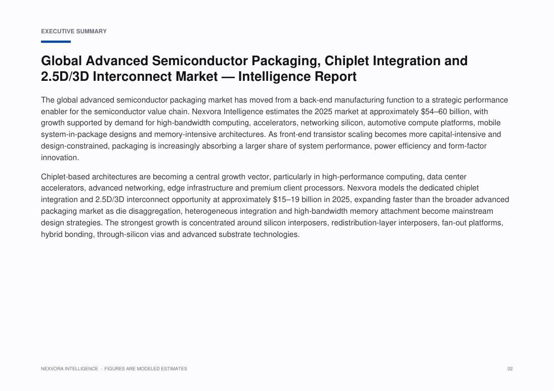
The global advanced semiconductor packaging market has moved from a back-end manufacturing function to a strategic performance enabler for the semiconductor value chain. Nexvora Intelligence estimates the 2025 market at approximately $•••–••• billion, with growth supported by demand for high-bandwidth computing, accelerators, networking silicon, automotive compute platforms, mobile system-in-package designs and memory-intensive architectures. As front-end transistor scaling becomes more capital-intensive and design-constrained, packaging is increasingly absorbing a larger share of system performance, power efficiency and form-factor innovation.
Chiplet-based architectures are becoming a central growth vector, particularly in high-performance computing, data center accelerators, advanced networking, edge infrastructure and premium client processors. Nexvora models the dedicated chiplet integration and 2.5D/3D interconnect opportunity at approximately $•••–••• billion in 2025, expanding faster than the broader advanced packaging market as die disaggregation, heterogeneous integration and high-bandwidth memory attachment become mainstream design strategies. The strongest growth is concentrated around silicon interposers, redistribution-layer interposers, fan-out platforms, hybrid bonding, through-silicon vias and advanced substrate technologies.
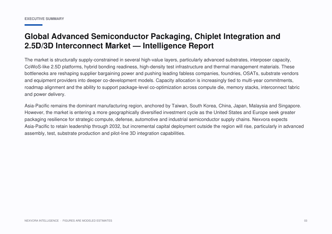
The market is structurally supply-constrained in several high-value layers, particularly advanced substrates, interposer capacity, CoWoS-like 2.5D platforms, hybrid bonding readiness, high-density test infrastructure and thermal management materials. These bottlenecks are reshaping supplier bargaining power and pushing leading fabless companies, foundries, OSATs, substrate vendors and equipment providers into deeper co-development models. Capacity allocation is increasingly tied to multi-year commitments, roadmap alignment and the ability to support package-level co-optimization across compute die, memory stacks, interconnect fabric and power delivery.
Asia-Pacific remains the dominant manufacturing region, anchored by Taiwan, South Korea, China, Japan, Malaysia and Singapore. However, the market is entering a more geographically diversified investment cycle as the United States and Europe seek greater packaging resilience for strategic compute, defense, automotive and industrial semiconductor supply chains. Nexvora expects Asia-Pacific to retain leadership through 2032, but incremental capital deployment outside the region will rise, particularly in advanced assembly, test, substrate production and pilot-line 3D integration capabilities.
Specific figures are hidden in this free preview. Unlock the report to see all modeled market sizes, forecasts and growth rates.
What this report covers.
Strategic market outlook for high-density packaging architectures, heterogeneous integration and next-generation interconnect platforms, 2025–2032
Who this report is for.
- Corporate strategy, planning and M&A teams evaluating the market
- Investors, private equity and venture teams sizing the opportunity
- Product, marketing and go-to-market leaders
- Consultants and analysts building the competitive picture
- Executives planning market entry, expansion or investment
How this report is built.
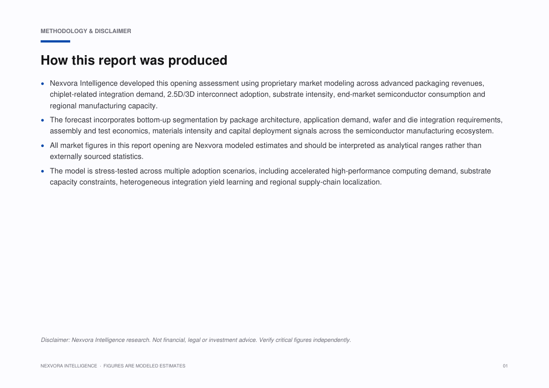
Nexvora Intelligence developed this opening assessment using proprietary market modeling across advanced packaging revenues, chiplet-related integration demand, 2.5D/3D interconnect adoption, substrate intensity, end-market semiconductor consumption and regional manufacturing capacity.
The forecast incorporates bottom-up segmentation by package architecture, application demand, wafer and die integration requirements, assembly and test economics, materials intensity and capital deployment signals across the semiconductor manufacturing ecosystem.
All market figures in this report opening are Nexvora modeled estimates and should be interpreted as analytical ranges rather than externally sourced statistics.
The model is stress-tested across multiple adoption scenarios, including accelerated high-performance computing demand, substrate capacity constraints, heterogeneous integration yield learning and regional supply-chain localization.
What's inside — a number-free look.
A full outline of the figures and tables you'll get. Specific data, market sizes and forecasts are unlocked with purchase.
List of Figures
- Figure 1: Market Overview and Structure — Advanced Semiconductor Packaging, Chiplet Integration and 2.5D/3D Interconnect
- Figure 2: Market Size and Forecast Framework — Advanced Semiconductor Packaging, Chiplet Integration and 2.5D/3D Interconnect
- Figure 3: Value Chain and Ecosystem Analysis — Advanced Semiconductor Packaging, Chiplet Integration and 2.5D/3D Interconnect
- Figure 4: Market Dynamics — Drivers, Restraints and Opportunities — Advanced Semiconductor Packaging, Chiplet Integration and 2.5D/3D Interconnect
- Figure 5: Segment Contribution Analysis — Advanced Semiconductor Packaging, Chiplet Integration and 2.5D/3D Interconnect
- Figure 6: Regional Market Landscape — Advanced Semiconductor Packaging, Chiplet Integration and 2.5D/3D Interconnect
- Figure 7: Country-level Opportunity Mapping — Advanced Semiconductor Packaging, Chiplet Integration and 2.5D/3D Interconnect
- Figure 8: Competitive Positioning Matrix — Advanced Semiconductor Packaging, Chiplet Integration and 2.5D/3D Interconnect
- Figure 9: Market Share of Leading Players — Advanced Semiconductor Packaging, Chiplet Integration and 2.5D/3D Interconnect
- Figure 10: Adoption and Penetration Trends — Advanced Semiconductor Packaging, Chiplet Integration and 2.5D/3D Interconnect
- Figure 11: Technology and Innovation Landscape — Advanced Semiconductor Packaging, Chiplet Integration and 2.5D/3D Interconnect
- Figure 12: Pricing and Business Model Analysis — Advanced Semiconductor Packaging, Chiplet Integration and 2.5D/3D Interconnect
- Figure 13: Investment, Funding and M&A Landscape — Advanced Semiconductor Packaging, Chiplet Integration and 2.5D/3D Interconnect
- Figure 14: Regulatory and Policy Framework — Advanced Semiconductor Packaging, Chiplet Integration and 2.5D/3D Interconnect
- Figure 15: Porter's Five Forces Analysis — Advanced Semiconductor Packaging, Chiplet Integration and 2.5D/3D Interconnect
- Figure 16: PESTLE Analysis — Advanced Semiconductor Packaging, Chiplet Integration and 2.5D/3D Interconnect
- Figure 17: Growth Opportunity Heat Map — Advanced Semiconductor Packaging, Chiplet Integration and 2.5D/3D Interconnect
- Figure 18: Future Outlook and Strategic Roadmap — Advanced Semiconductor Packaging, Chiplet Integration and 2.5D/3D Interconnect
List of Tables
- Table 1: Market Segmentation Overview — Advanced Semiconductor Packaging, Chiplet Integration and 2.5D/3D Interconnect
- Table 2: Segment Definitions and Scope — Advanced Semiconductor Packaging, Chiplet Integration and 2.5D/3D Interconnect
- Table 3: Regional and Country Coverage Summary — Advanced Semiconductor Packaging, Chiplet Integration and 2.5D/3D Interconnect
- Table 4: Key Company Profiles and Offerings — Advanced Semiconductor Packaging, Chiplet Integration and 2.5D/3D Interconnect
- Table 5: Competitive Benchmarking Matrix — Advanced Semiconductor Packaging, Chiplet Integration and 2.5D/3D Interconnect
- Table 6: Product and Service Portfolio Mapping — Advanced Semiconductor Packaging, Chiplet Integration and 2.5D/3D Interconnect
- Table 7: Market Drivers, Restraints and Trends — Advanced Semiconductor Packaging, Chiplet Integration and 2.5D/3D Interconnect
- Table 8: Strategic Initiatives and Developments — Advanced Semiconductor Packaging, Chiplet Integration and 2.5D/3D Interconnect
- Table 9: Partnerships and Collaborations — Advanced Semiconductor Packaging, Chiplet Integration and 2.5D/3D Interconnect
- Table 10: Research Assumptions and Limitations — Advanced Semiconductor Packaging, Chiplet Integration and 2.5D/3D Interconnect
- Table 11: Data Sources and References — Advanced Semiconductor Packaging, Chiplet Integration and 2.5D/3D Interconnect
- Table 12: Report Scope and Coverage Summary — Advanced Semiconductor Packaging, Chiplet Integration and 2.5D/3D Interconnect
A look at the pages.
107 pages · 20 sections · charts & tables
A genuine peek at the opening pages. Unlock to read every page in full.
6 of 107 pages shown
Turn this market into a plan for your business.
Answer a few quick questions and unlock a personalised operational read — your maturity score, prioritised focus areas and quick wins — mapped to where this market is heading. Result delivered instantly and emailed to you.
- Maturity score & prioritised focus areas
- Practical quick wins and a recommended next step
Questions, answered.
How big is the Global Advanced Semiconductor Packaging, Chiplet Integration and 2.5D/3D Interconnect Market?
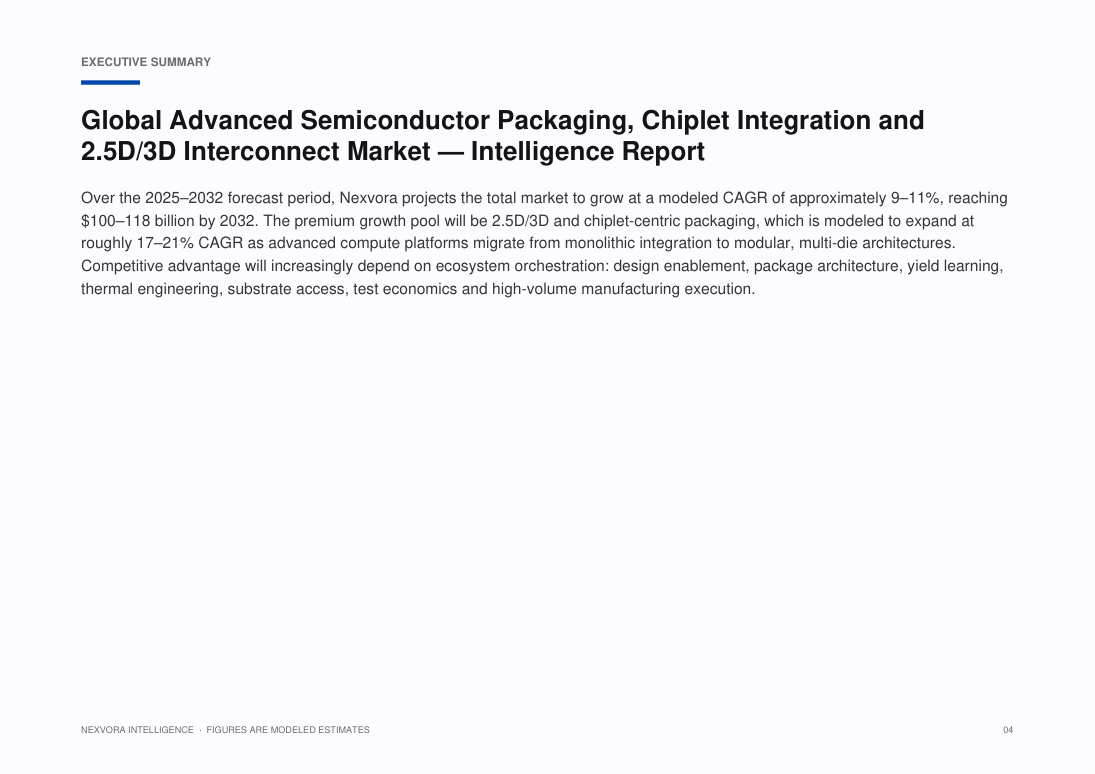
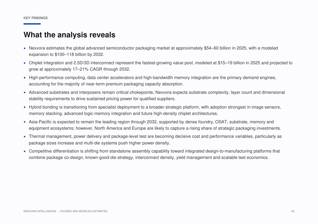
Nexvora models the Global Advanced Semiconductor Packaging, Chiplet Integration and 2.5D/3D Interconnect Market at approximately $54–60 billion, 2025. Full market sizing, segmentation and forecasts are inside the report (modeled estimate).
What is the growth rate (CAGR) of the Global Advanced Semiconductor Packaging, Chiplet Integration and 2.5D/3D Interconnect Market?
The Global Advanced Semiconductor Packaging, Chiplet Integration and 2.5D/3D Interconnect Market is projected to grow at a CAGR of about 9–11%, 2025–2032 over the forecast period — a Nexvora modeled estimate detailed across the report's 20 sections.
What does this report include?
A complete market intelligence report — market sizing and forecasts, segmentation, regional and industry analysis, competitive landscape, trends, and strategic recommendations across 20 sections.
How do I access it after purchase?
Instantly, in your secure online viewer. Reports are view-only and available on any device from your library.
Are the figures sourced?
Quantitative figures are Nexvora modeled estimates unless explicitly cited to a referenced source within the report.
Can I buy access for my team?
Yes — add user seats at checkout, or subscribe for bulk access across multiple reports.
Nexvora Intelligence research report. All quantitative figures are modeled estimates — not audited data. Not financial or investment advice.
More market reports
Keep exploring intelligence in this and related sectors.

Global Humanoid Robotics Market — Industrial & Service Automation Intelligence Report

Global Counter-Drone Defense, C-UAS Detection and Autonomous Airspace Security Market — Intelligence Report

Global Autonomous Mining, Electrified Haulage and Critical Minerals Digital Operations Market — Intelligence Report